Social Implementation
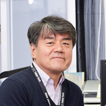
Takayuki Ohba
Specially Appointed Professor
SemiconductorsProcess IntegrationThermal EngineeringPlatelets Bio GeneratorSemiconductor -Agriculture Concurrent Engineering
Biography
Dr. Takayuki Ohba is a Professor at Tokyo Institute of Technology (Tokyo Tech) from 2013 and The University of Tokyo from 2004 to 2013, respectively. He was worked at semiconductor department of Fujitsu Limited from 1984 and received his Ph.D. degree from Tohoku University (Electrical Communication) in 1995.
Expectations for WRHI
Technology implementation to industry with flexible and continuous support
Research Projects
-
Tera Scale 3D IC, Wafer Multi-Stack, Advanced Packaging, Bumpless Interconnects, Ultra-Thinning, Cooling Device, Thermal Management
-
Heterogeneous and Functional Integration R&D
The development of large scale 3D integration technology for Tera-byte memory, ultra-small system module, bio-devices, and functional sensor to recognize thoughts of plant are being conducted by research platform in cooperation with industries, so-called WOW Alliance.
Topics
-
Press Conference, High Performance Closed-Channel Cooling System Using Multi-channel Electro-osmotic Flow pumps for 3D-ICs, Dec 9, 2013.
-
Press Conference, Ultra-Thinning of 300-mm Wafer Down to 4-µm Thickness-Proven by DRAM, applicable for the next Three Dimensional Large Scale Memories-, June 20, 2014
-
Press Conference, Reducing 30% of Thermal Resistance by WOW Technology for 3D DRAM Application, May 8, 2017
| 1984 - 2003 | Fujitsu Limited |
|---|---|
| 1994 - 1995 | Tohoku University, Ph.D. |
| 2004 - 2013 | The University of Tokyo, Professor |
| 2014 - | Tokyo Institute of Technology,Professor(Specially Appointed) |
| 2018 | Conference Award, IEEE iMPACT |
|---|---|
| 2020 | the 2020 Best Papers Awards for the IEEE Transactions on Components, Packaging and Manufacturing Technology |
| 2013 | “Advanced wafer thinning technology and feasibility test for 3D integration, Microelectronic Engineering, Volume 107, July 2013, Pages 65–71 “Impact of Thermomechanical Stresses on Bumpless Chip in Stacked Wafer Structure, Jpn. J. Appl. Phys. 52 (2013) 05FE01 “Tera-Scale Three-Dimensional Integration (3DI) using Bumpless TSV Interconnects,” IEICE Technical Report, Aug. 1, 2013. “Wafer level three-dimensional integration (3DI) using bumpless TSV interconnects for tera-scale generation,” IEEE Semiconductor Conference Dresden-Grenoble (ISCDG), 2013 International, pp. 1-4, 2013, DOI: 10.1109/ISCDG.2013.6656328 “High Performance Closed-Channel Cooling System Using Multi-channel Electro-osmotic Flow pumps for 3D-ICs”, IEEE International Electron Devices Meeting (IEDM), Washington DC, 2013, pp. 480-483. “Influence of Wafer Thinning Process on Backside Damage in 3D Integration,” IEEE Int’l 3D Sys. Integration Conf. 2013 |
|---|---|
| 2014 | “An Innovative Bumpless Stacking with Through Silicon Via for 3D Wafer-On-Wafer (WOW) Integration”, IEEE Electronic Components and Technology Conference (ECTC), Orlando, 2014, pp.1853-1856. “Ultra Thinning down to 4-μm using 300-mm Wafer proven by 40-nm Node 2Gb DRAM for 3D Multi-stack WOW Applications”, IEEE Symp. on VLSI Technol., Honolulu, pp.26-27, 2014. “Impact of Thermomechanical Stresses on Ultra-thin Si Stacked Structure,” IEEE Int’l 3D Sys. Integration Conf., Cork, 2014. “Vacancy-type defects induced by grinding of Si wafers studied by mono-energetic positron beams”, J. Appl. Phys 116, 134501 (2014) “Observation of lattice spacing fluctuation and strain undulation around through-Si vias in wafer-on-wafer structures using X-ray microbeam diffraction”, Jpn. J. Appl. Phys. 53, 05GE03 (2014). “Impact of back-grinding-induced damage on Si wafer thinning for three-dimensional integration,” Jpn. J. Appl. Phys., vol. 53, 05GE04, 2014. |
| 2015 | “Review of Wafer-Level Three-Dimensional Integration (3DI) using Bumpless Interconnects for Tera-Scale Generation,” IEICE Electronics Express, vol. 12 (7), pp. 1-14, DOI: 10.1587/elex.12.20150002 (2015). “A Robust Wafer Thinning down to 2.6-μm for Bumpless Interconnects and DRAM WOW Applications”, IEDM2015 Tech. Dig., 190 (2015) |
| 2016 | “Warpage-free Ultra-Thinning ranged from 2 to 5-μm for DRAM Wafers and Evaluation of Devices Characteristics”, ECTC2016., 1461 (2016) “Production-Worthy WOW 3DI Technology using Bumpless Interconnects and Ultra-Thinning Processes,” IEEE VLSI Symp., pp. 184-185, 2016. “A BIOREACTOR FOR PLATELET GENERATION WITH HIGH PRODUCTIVITY THROUGH NARROW SLITS OF PDMS”, 20th International Conference on Miniaturized Systems for Chemistry and Life Sciences, 2016, p. 1025-1026 “Laser Dicing for Higher Chip Productivity”, Proc. Int ‘ l Microsystems, Packaging, Assembly and Circuit Technol. Conf. (IMPACT), Taiwan, pp. 242-244, 2016. |