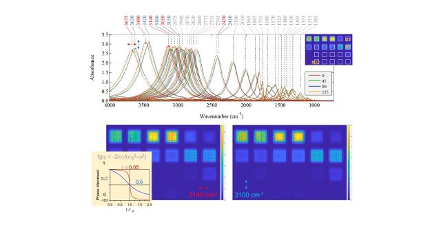
The four polarisation method is adopted for measurement of molecular orientation in dielectric nanolayers of metal-insulator-metal (MIM) metamaterials composed of gold nanodisks on polyimide and gold films. Hyperspectral mapping at the chemical finger printing spectral range of 4–20 μμm was carried out for MIM patterns of 1–2.5 μμm period (sub-wavelength). Overlay images taken at 0, π/4, π/2, 3π/4 orientation angles and subsequent baseline compensation are shown to be critically important for the interpretation of chemical mapping results and reduction of spurious artefacts. Light field enhancement in the 60-nm-thick polyimide (I in MIM) was responsible for strong absorption at the characteristic polyimide bands. Strong absorbance A at narrow IR bands can be used as a thermal emitter (emittance E=1−R), where R is the reflectance and A=1−R−T, where for optically thick samples the transmittance is T=0
Hyperspectral mapping for measurement of molecular orientation in dielectric nanolayers of metal-insulator-metal (MIM) metamaterials composed of gold nanodisks on polyimide and gold films
WRHI Newsおすすめ
Published
(School of Materials and Chemical Technology / Dr. Junko Morikawa and Dr. Saulius Juodkazis)
“Hyperspectral Molecular Orientation Mapping in Metamaterials”
Appl. Sci. (DOI:10.3390/app11041544)
For details, click here.
<Abstract>